
The main goal of VLSI technology is to pack billions of transistors onto a single chip to create advanced devices and system-on-a-chips. Several sectors, including data centers, telecommunications, consumer electronics, automotive, defense, and industrial automation, among others, depend extensively on the chips. Manufacturing these small chips, which are made of billions of transistors and their interconnects to form very complex circuitry.
For a chip to be launched into the consumer market, it must meet the standards of area, performance, and power. As a result, depending on the application, the area and power of a design may vary from one to another. However, all designs must consider performance as a critical component.
In digital design, timing analysis is a crucial stage, particularly in VLSI (Very Large Scale Integration), where it ensures that a device or system works correctly at the desired clock frequency. It ensures that every path satisfies the necessary timing requirements, allowing data to flow across the circuit free of violations. To ensure that the circuit meets requirements in terms of area, power and speed, reliability, and functional criteria, there are various types of essential factors to take into account during timing analysis in VLSI design. Operating conditions are among them, and in addition, RC parasitics during the timing analysis, are the most significant elements. The significance of these parasitics, in affecting the timing, power, and performance of a VLSI design increases as technology progresses to nanoscale nodes in terms of overall chip behavior and signal integrity.
Also read: What is a Buffer in VLSI?
The sources for the RC parasitics are Interconnect Resistance and Interconnect Capacitance.
Interconnect Capacitance
Interconnect wires can hold electrical charge because they are placed close to each other. When a signal moves through a wire, it acts like a surface that holds a lot of charge (Plate).
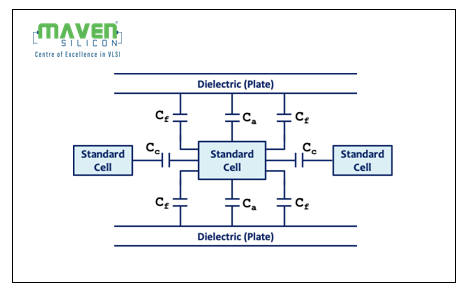

There can be three types of capacitance available in the designs. They are:
- Coupling Capacitance Cc = ε*T/S
- Area Capacitance per Unit length Ca = ε*W/H
- Fringe Capacitance Cf
The values of the capacitances are dependent on the below parameters
- Dielectric Constant (ε)
- Width of Metal (W)
- Thickness of Metal (T)
- Spacing between the metals (S)
- Thickness of Dielectric (ILD –Interlayer Dielectric) (H)
Also read: 3D Integration in VLSI Circuits
Interconnect Resistance
All materials resist the flow of electricity to some extent. Conductors have low resistance, materials like highly doped silicon have moderate resistance, and insulators have very high resistance. In CMOS circuits, different materials are used based on their level of resistance.
“Resistivity depends on the material of the metal layer. Resistance is directly proportional to delay; when the resistance increases, the delay also increases.”
Resistance per unit length = p*W/T
- Resistivity of the metal layer (p)
- Width of Metal (W)
- Thickness of Metal (T)
By considering the above interconnect parasitics, the RC corners (combinations of R and C) will be taken for timing analysis.
RC corners refer to different combinations of resistance (R) and capacitance (C) values used during timing analysis and circuit simulation. These variations are introduced to account for the inherent manufacturing process variations, temperature changes, and voltage fluctuations that can affect the performance of an integrated circuit (IC).
Why RC Corners in Timing Analysis?
The RC parasitics (resistance and capacitance) associated with interconnects and transistors influence signal propagation delay in a chip. To ensure robust design, designers use different RC corners, typically grouped into:
- Metal layers are connected with the help of via’s. Between two metal layers, there is a material known as dielectric.
- All the metals as per the technology have to follow certain design rules and the rules are the minimum width of the metal layer and minimum spacing between two metal layers.
Based on the above parameters, two RC extraction corners are defined which are called conventional RC corners.
- Cbest (also known as Cmin) – minimizes capacitance, maximizes the resistance
- Cworst (also known as Cmax) – maximizes capacitance, minimizes the resistance
Also read: What is Skew in VLSI?
Cell delay is calculated as the product of RC i.e., (R*C). The connection delay plays a major role in a timing path below the 90nm node. At a timing path’s endpoint, the coupling capacitance component (Cc) in the net delay can alter the slack levels. RC corners have been divided into two types, depending upon the contribution of each component like ground capacitance (Cg) and the coupling capacitance (Cc). Based on this, the foundry came up with two more additional corners on top of conventional corners.
- RCbest (XTALK corner) – Cc is max and Cg x R is min.
- RCworst (Delay corner) – Cc is min and Cg x R is max.
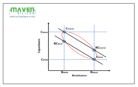
The below figure shows the graphical representation of RC parasitic corners: Parasitic capacitance and parasitic resistance are the values that the foundry will provide in the PDK for the previously mentioned properties, such as Cbest, Cworst, RCbest, and RCworst. These are the maximum and minimum reference values for resistance and capacitance, respectively. These values are not design-specific since they change according to the length of the metal layers.
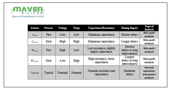
1) Cbest:
- This corner will have the lowest capacitance and highest resistance and will be also called as Cmin
- Results in the shortest delay for paths with short nets, ideal for min-path analysis.
2) Cworst:
- This is the corner where the capacitance will be high and the interconnect resistance will be lower than the typical corner and this corner will be called as the Cmax
- Results in the longest delay for paths with short nets, useful for max-path analysis.
3) RCbest:
- Refers to corners that minimize the interconnect RC product, also called RC-min
- Typically results from smaller etch widths, increasing trace width, which lowers resistance but slightly increases capacitance.
- Results in the shortest path delay for long interconnects, ideal for min-path analysis.

Example: Assume a VLSI design with a long connecting wire. The wire is widened in the RCbest corner to reduce resistance, which allows electrons to pass through more readily and speeds up signal transmission. Because a larger wire can hold more charge, the greater width somewhat increases capacitance; nevertheless, the reduced resistance is more significant and leads to quicker signal timing. This scenario is commonly employed in min-path analysis for calculating the circuit’s traversal speed of signals. This corner will be used for performing the timing analysis for the faster signals.
4) RCworst:
- Refers to corners that maximize the interconnect RC product, also known as RC-max
- Typically results from larger etch widths, decreasing trace width, which increases resistance but reduces capacitance.
- Results in the longest path delay for long interconnects, useful for max-path analysis.
Consider the same length connecting wire, but narrower at the RCworst corner to increase resistance. Higher resistance slows the current and causes the signal to travel more slowly. Although reduced width reduces capacitance (since a thinner wire stores less charge), increased resistance dominates, resulting in delayed signal timing. This is used for maximum-path analysis, determining how long signals can travel across the circuit in the worst-case scenario. RCworst is useful for ensuring that the circuit will match timing requirements even in the most adverse situations, such as in paths with lengthy interconnects or under high-resistance scenarios.
5) Typical:
Represents the nominal values for interconnect resistance and capacitance.
Summary of RC Corners in addition to PVT Corners
As stated in this article, the following RC corners, in addition to the PVT corners, can be used for time analysis.