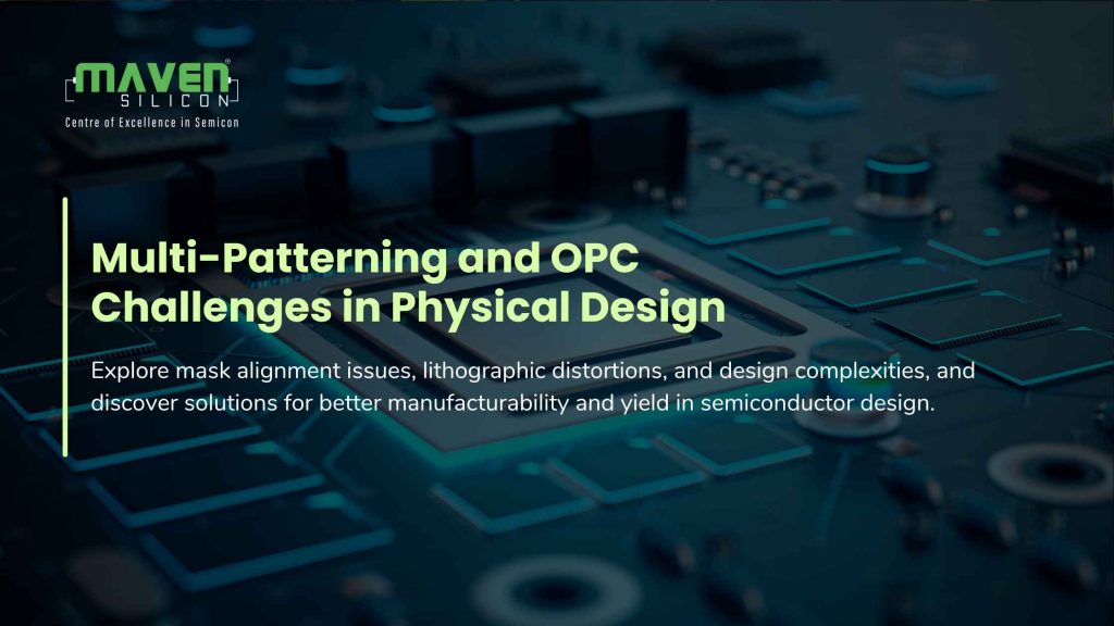
Introduction
As technology advances day by day, it becomes increasingly challenging to transfer patterns onto silicon wafers with high accuracy. To address these challenges, traditional lithography is no longer suitable for fabricating complex designs due to its wavelength limitations. To overcome these challenges, Multi-Patterning (MP) and Optical Proximity Correction (OPC) techniques are extensively used. These techniques ensure that the design layout generated during the Physical Design stage can be accurately fabricated while maintaining yield, performance, and manufacturability.
Why Do We Have to Use Multi-Patterning & OPC?
Impact on Physical Design
The Physical Design (PD) process consists of various stages like floorplanning, placement, clock tree synthesis (CTS), and routing. During these stages, power, performance, and area requirements must be considered. As the technology node shrinks, the constraints for the layout become more crucial due to lithographic limitations. Multi-patterning (MP) is a technique needed when the pitch becomes smaller than the resolution limit of lithography tools. This requires multiple exposures to correctly define shapes. Optical Proximity Correction (OPC) compensates for pattern distortions that occur during photolithography, ensuring the fabricated wafer matches the intended PD layout.
How Are These Used in Fabrication?
Design Rule Constraints in Physical Design
At advanced technology nodes, Design Rule Constraints are defined strictly due to multi-patterning limitations. Color-aware routing tracks are defined during the routing stage. Violating multi-patterning constraints can lead to misalignment in the masks, which affects manufacturing yield.
Mask Generation and OPC Implementation
After completing the Physical Design Signoff process, the layout is provided for mask generation. Different OPC techniques are then applied:
- Rule-Based OPC: Applies predefined rules to correct distortions.
- Model-Based OPC: Uses lithography simulations to predict pattern distortions and optimize mask shapes.
- Inverse Lithography (ILT): An advanced, AI-driven technique that enhances mask accuracy.
Lithography and Multi-Patterning in Fabrication
- Double Patterning (DPT): Uses two masks for a single layout, improving feature resolution.
- Self-Aligned Quad Patterning (SAQP): Ensures the accuracy of the interconnect routing of critical nets.
- Post-Fabrication Verification: Ensures that the printed wafer matches the layout extracted from the physical design using lithographic simulations.
Advantages of Multi-Patterning & OPC in Physical Design
- Ensures all designs in advanced technology nodes maintain design accuracy.
- Helps meet DRC (Design Rule Check) rules by ensuring correct feature alignment.
- Prevents fabrication-induced distortions that can alter interconnect parasitics, leading to timing distortions.
- Improves yield and manufacturability.
- Enables high-density routing and interconnect layers.
Conclusion
Multi-Patterning and OPC techniques are critical in the journey from Physical Design to Fabrication. As these techniques become more complex, AI-driven OPC tools are being explored to reduce the need for multi-patterning. However, until EUV (Extreme Ultra Violet) lithography becomes fully mature, multi-patterning-aware physical design methodologies will remain essential for ensuring successful timing closure, area optimization, and manufacturability in advanced semiconductor nodes.