Introduction
When Gordon Moore, co-founder of Intel, made his famous observation in 1965, he predicted that the number of transistors on a microchip would double roughly every two years, leading to ever-increasing performance and smaller, cheaper chips. This became the famous Moore’s Law, and for decades, it guided the rapid advancement of semiconductor technology. As transistors became smaller, chips became faster and more efficient, meeting the growing demands of everything from computers to smartphones.
However, we’re starting to reach the limits of Moore’s Law. As transistor sizes shrink to the 7nm, 5nm, and even 3nm nodes, it’s becoming harder to make these transistors smaller without running into significant challenges like heat dissipation, leakage currents, and manufacturing complexities. At these tiny sizes, the physical properties of the materials start to behave in unexpected ways, making it difficult to continue on the same trajectory of progress.
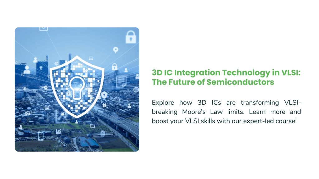
So, what happens when Moore’s Law begins to stagnate? The answer lies in 3D IC (Integrated Circuit) technology which is an innovative approach that promises to push semiconductor development beyond these physical limits.
To understand 3D IC technology, let’s use an analogy. Imagine a city full of standalone houses. Each house represents an individual semiconductor chip, and the space between them represents the distance required for data transfer or communication between these chips. In the traditional 2D chip design, the chips are placed next to each other on a flat surface (on a PCB, in general), just like houses spread out in a city.
Now, imagine if instead of building separate houses, we built apartments where multiple floors are stacked on top of each other. This is similar to 3D IC technology, where multiple layers of semiconductor chips are stacked vertically, instead of spreading them out on a single plane. By stacking chips like floors in an apartment building, we can utilize the same physical area more efficiently.
Why is this better?
Well, just like apartments offer more living space in a smaller footprint compared to standalone houses, 3D ICs offer greater performance with reduced processing power consumption, in a smaller area. By stacking multiple layers of chips, we can increase the packaging density of the transistors.
Now let’s try to understand how 3D ICs Work:
In traditional semiconductor designs, chips are laid out on a single plane (2D). The signal paths (interconnections) between different parts of the chip can become long and complicated, which leads to problems like signal delay (longer time for signals to travel across the chip) and power loss (because longer connections require more power). These issues become more significant as chips get smaller.
3D IC technology tackles these problems by stacking layers of chips on top of each other. These layers are interconnected through vertical interconnects small pathways called Through-Silicon Vias (TSVs). Think of TSVs like tunnels that connect different floors in an apartment building. These vias allow data to move between the stacked layers much faster and more efficiently than traditional horizontal connections in a 2D chip.
The key components that can be stacked in a 3D IC design include:
Logic chips, Memory chips, Specialized chips.
By stacking these different types of chips together, we can create systems with more processing power, faster data transfer speeds, and reduced power consumption all within a smaller area than traditional 2D IC designs. This is especially useful in modern applications like smartphones, high-performance computing, and Internet of Things (IoT) devices, where space, performance, and power efficiency are critical.
Why 3D ICs?
Improved Performance:
By stacking chips, we reduce the distance data needs to travel. This results in faster data transfer between the layers, leading to improved performance. For example, integrating a processor layer and a memory layer in close proximity eliminates the bottleneck of accessing memory, which is often the slowest part of a computer.
Reduced Power Consumption:
Shorter interconnections mean less energy is required to transfer data. This is particularly important in mobile devices where power efficiency is crucial for battery life.
Smaller Form Factor:
With 3D ICs, we can fit more components into the same area. Just like an apartment complex can house more people in the same land area as a collection of standalone houses, 3D ICs allow for more processing power in a smaller physical space. This compact design is key for mobile and wearable devices where space is at a premium.
Heterogeneous Integration:
In traditional designs, all the components are integrated on the same chip. With 3D ICs, we can combine different types of chips in the same stack such as logic, memory, and specialized sensors allowing for a more efficient, tailored system design. For example, you could have a processing layer on top of a memory layer, with sensors integrated within the same stack for a specific application like autonomous vehicles or smart devices.
Challenges of 3D IC Technology:
While the benefits are discussed, there are still challenges to overcome in the development and deployment of 3D ICs:
Thermal Management:
Stacking multiple layers of chips increases the heat generated by the circuit. Efficient thermal management is crucial to ensure that the device doesn’t overheat and fail. Researchers are developing new cooling techniques to handle this issue. There are EDA tools available to analyze the heat distribution on the entire chip and identify the thermal hotspots in early stages of the design itself, so that we can handle the thermal issues before going for fabrication.
Manufacturing Complexity:
The process of stacking and aligning multiple layers of chips is more complex than traditional 2D designs. Creating small and reliable Through-Silicon Vias (TSVs) is difficult, and ensuring each layer functions properly without defects adds to the complexity.
Cost:
The process of creating 3D ICs is more expensive than traditional 2D ICs, primarily due to the advanced manufacturing techniques required. As the technology matures, costs are expected to decrease, but for now, this remains a barrier to widespread adoption.
Future scope of 3D ICs
Despite the challenges, 3D ICs hold immense potential for the future and present of semiconductor technology. With increasing demand for more powerful, compact, and energy-efficient devices, 3D ICs offer a path forward as traditional 2D designs reach their physical limits.
In the coming years, we can expect to see 3D IC technology play a critical role in the development of Artificial intelligence (AI) and machine learning applications, where large amounts of data need to be processed quickly, Mobile devices, where area and power efficiency are important and High-performance computing systems, where performance and energy efficiency are key.
To summarize, 3D IC integration is a key breakthrough in pushing past the limits of Moore’s Law. By stacking chips on top of each other, it makes devices faster, more power-efficient, and smaller. This technology doesn’t just improve how we build chips today, it has the power to completely change how we use electronics in the future. As 3D ICs keep improving, they could lead to faster, more powerful gadgets that are more compact and energy-efficient, opening up exciting possibilities for the next generation of tech keeping Moore’s law, valid even in future.