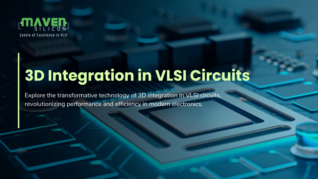
Introduction to 3D Integration in VLSI Circuits
Over the years, the field of VLSI circuits has witnessed remarkable advancements. One such breakthrough is the advent of 3D integration, which has revolutionized the way integrated circuits are designed and manufactured. In this article, we will explore the concept of 3D integration in VLSI circuits, its benefits, various techniques employed, advancements in technology, future trends, and a comparison between 2D and 3D integration. So, let’s dive into the fascinating world of 3D integration.
Benefits of 3D Integration in VLSI Circuits
3D integration offers a plethora of advantages over traditional 2D integration techniques. Firstly, it allows for a significant reduction in the overall size of the integrated circuit, making it possible to pack more functionality into a smaller footprint. This miniaturization leads to improved performance and power efficiency. Additionally, 3D integration enables the integration of heterogeneous technologies, such as combining logic and memory elements on the same chip. This integration of different functionalities on a single chip eliminates the need for complex and power-hungry interconnects, resulting in faster and more reliable circuits.
Another major advantage of 3D integration is the improved interconnect density. By stacking multiple layers of circuitry, the length of interconnects is drastically reduced, minimizing signal propagation delays and improving overall system speed. Moreover, 3D integration allows for increased functionality by providing more routing resources, enabling the design of complex circuits that were previously unattainable using 2D integration. These benefits make 3D integration a compelling choice for modern VLSI circuits.
Also read: How to Learn VLSI from scratch?
Types of 3D Integration Techniques
There are several techniques used for 3D integration in VLSI circuits, each with its unique characteristics and considerations. Let’s take a closer look at some of the most prominent techniques:
Through-Silicon Via (TSV)
This technique involves creating vertical interconnects that pass through the silicon substrate, connecting different layers of the integrated circuit. TSV offers high interconnect density and low parasitic capacitance, making it suitable for high-performance applications.
Wafer-to-Wafer (W2W) Bonding
W2W bonding involves bonding two or more separate wafers together, creating a multi-layered structure. This technique allows for the integration of circuits fabricated on different wafers, enabling the combination of diverse technologies on a single chip.
Die-to-Wafer (D2W) Bonding
In D2W bonding, individual dies are bonded onto a pre-fabricated wafer, creating a multi-layered structure. This technique is particularly useful for integrating specialized circuits, such as memory, into a larger system.
Monolithic 3D Integration
This technique involves fabricating multiple layers of transistors on a single wafer, using specialized processes like epitaxial growth or layer transfer. Monolithic 3D integration offers the highest interconnect density and performance but requires complex fabrication processes.
These techniques, along with their variations and combinations, provide flexibility and scalability in 3D integration, catering to the diverse needs of VLSI circuit designers.
Advancements in 3D Integration Technology
In recent years, significant advancements have been made in 3D integration technology, enhancing its capabilities and expanding its applications. One notable advancement is the refinement of TSV manufacturing processes, leading to improved TSV density and reliability. This has paved the way for the integration of more complex circuits and higher-performance systems.
Another key development is the emergence of new materials and bonding techniques that enable more robust and reliable wafer-to-wafer and die-to-wafer bonding. These advancements have made it possible to integrate diverse technologies and functionalities on a single chip, opening up new possibilities for innovative system designs.
Furthermore, the introduction of advanced thermal management techniques in 3D integration has addressed the heat dissipation challenges inherent in densely packed circuits. This has improved the overall reliability and lifespan of 3D integrated circuits, making them a viable option for a wide range of applications, including high-performance computing, mobile devices, and Internet of Things (IoT) devices.
Also read: Machine Learning in VLSI
Future Trends in 3D Integration in VLSI Circuits
The future of 3D integration in VLSI circuits looks promising, with several exciting trends on the horizon. One such trend is the integration of emerging technologies, such as nanoscale devices and sensors, into 3D integrated circuits. This integration will enable the development of more compact and efficient systems for applications like biomedical devices, wearable electronics, and autonomous vehicles.
Another future trend is the exploration of advanced packaging techniques, such as System-in-Package (SiP) and Chiplets, in conjunction with 3D integration. These packaging approaches complement 3D integration by providing a scalable and modular framework for integrating multiple chips and subsystems, further enhancing the flexibility and functionality of VLSI circuits.
Furthermore, research is underway to develop novel 3D integration architectures, such as the use of unconventional materials, vertical nanowires, and carbon nanotubes. These advancements hold the potential to push the boundaries of performance, power efficiency, and miniaturization in VLSI circuits, opening up new avenues for innovation in the semiconductor industry.
Also read: Opportunity and Challenges for VLSI in IoT Devices
Comparison of 2D and 3D Integration in VLSI Circuits
While 2D integration has been the dominant approach in VLSI circuit design for decades, the emergence of 3D integration has raised the question of whether it is a superior alternative. Let’s compare these two approaches based on various factors:
Size and Density
3D integration allows for a significant size reduction and higher interconnect density compared to traditional 2D integration.
Performance and Power Efficiency
3D integration offers improved performance and power efficiency due to shorter interconnect lengths and reduced parasitic capacitance.
Functionality and Flexibility
3D integration enables the integration of heterogeneous technologies, providing greater functionality and flexibility in circuit design.
Manufacturing Complexity and Cost
3D integration involves additional manufacturing steps and may require specialized equipment, making it more complex and potentially costlier than 2D integration.
Design and Testing Challenges
Designing and testing 3D integrated circuits can be more challenging due to increased complexity and the need for specialized tools and methodologies.
Future Scalability
3D integration offers greater potential for future scalability and integration of emerging technologies compared to 2D integration.
Based on these factors, it is evident that 3D integration holds significant advantages over 2D integration, especially in terms of performance, miniaturization, and functionality. However, the decision to adopt 3D integration depends on the specific requirements and constraints of the target application.
Also read: Why VLSI is Used?
Conclusion
In conclusion, 3D integration has emerged as a game-changing technology in the field of VLSI circuits. Its numerous benefits, including size reduction, improved performance, enhanced functionality, and future scalability, make it an attractive choice for modern semiconductor designs. With continued advancements in 3D integration techniques and the exploration of new materials and architectures, the future of VLSI circuits looks exciting and promising. As the demand for smaller, faster, and more powerful electronic devices continues to grow, 3D integration will play a pivotal role in shaping the semiconductor industry.
So, whether you are a circuit designer, a researcher, or an enthusiast, it is essential to stay abreast of the latest trends and developments in 3D integration. Embracing this technology opens up a world of possibilities and paves the way for innovative and groundbreaking advancements in the realm of VLSI circuits.
If you’re interested in exploring a career as a VLSI engineer, check out our Online VLSI Courses and take the first step towards an exciting and fulfilling career in the semiconductor industry.