What is Physical Design & Verification?
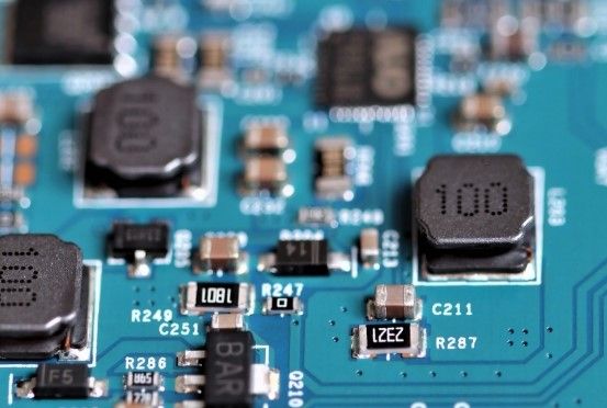
Physical design is the process of turning a design into manufacturable geometries. It transforms a circuit description into the physical layout, which describes the position of cells and routes for the interconnections between them. The purpose of the physical design of VLSI chips is to find a layout with minimal area, further, the total wire length has to be minimized. After the physical design is completed, the layout must be fully verified to ensure correct electrical and logical functionality. Some problems found during physical verification can be tolerated if their impact on chip yield is negligible. Therefore, at this stage, layout changes are usually performed manually by experienced design engineers.
Why is Physical Design and Verification important?
The physical design and verification are highly relevant as the right implementation is necessary to make the logical blueprint of the database system work. The physical design can optimize the query processing performance while simultaneously maintaining Data Integrity by preventing data redundancies. This optimal setup will also allow the database users to manage and access their data with more ease.
How to prepare for the Physical Design & Verification Interviews?
For the preparation for interviews, The engineers must go through various concepts and gain a thorough understanding on the below things. **1. Design flow and various steps in the design flow. 2. The tools used for various processes in the PD flow. 3. The different input and output files for each p
What is expected from the Physical Design & Verification interviews?
As mentioned above, the PD engineer should have thorough knowledge on various steps in the design and he should be able to the EDA Tools for those steps in the design flow.
Learning programs for Physical Design & Verification
The main steps in the PHYSICAL DESIGN flow are:
- Design netlist (after synthesis)
- Floor Planning
- Power planning
- Placement
- Clock Tree Synthesis(CTS)
- Routing
- Physical verification
- GDSII generation
- Core areas
- Periphery area, io ports, power ports, corner cells, filler cells
- Macro placement
- Placement blockages
- Power network synthesis
- If the number of routing tracks available for routing in one particular area is less than the required routing tracks then the area is said to be congested. There will be a limit to a number of nets that can be routed through a particular area.
- High Standard cell density in a small area
- Placement of standard cells near macros
- High pin density at the edge of macro
- Bad floorplan
- During IO optimization tool does buffer, So a lot of cells are placed in the core area
Each metal layer has a resistance value. When the current flows through the metal, then because of the resistance of the metal there will be a certain amount of voltage drop. This is called an IR drop. If the resistance is more then the drop is also more.
- Synchronous clocks: Same source for the clock input for all the flipflops or the constant phase difference between the main clock and generated clock.
- Asynchronous clocks: Different clock sources or no constant phase difference
Clock Tree Synthesis is done to ensure the clock signal reaches all the flip-flops with no skew difference.
- Clock gating.
- Multi Vth and Multi Vdd
- Power gating
- Pipelining
- Input re-ordering
- logic Re-Structuring
- Optimizing the operating system
- Global routing: just you can see the lines without vias.
- Detailed Routing: Physical nets with vias
- More Space
- Shielding
- Order the nets such that timing dependent/timing window overlap nets are far from each other
- Increase the drive strength of the victim's net
- Having differential signal lines
- Process
- Voltage
- Temperature
Conclusion
The task of VLSI physical design is to produce the layout of an integrated circuit. New performance requirements are becoming increasingly dominant in today’s sub-micron regimes requiring new physical design algorithms. Anyone who wants to pursue a career in Physical design and Verification must learn and master it by practicing the physical design and verification interview questions. These interview questions and answers will help you prepare well for the physical design job roles and bag a good VLSI job opportunity.
More VLSI Interview Questions


