Maven silicon

Courses / Job Oriented / Advanced VLSI Design and DFT Course - [VLSI DFT]

Advanced VLSI Design and DFT Course - [VLSI DFT]

Set yourself up for success with the advanced VLSI DFT course

Maven silicon

Superior Training Methodology

App-based courses

24x7 Online Support & Lab Access

250+ Industry partners

5000+ Alumni Shining Globally

Industry Standard EDA Tools

Highly Expert Trainers

Superior Training Methodology

App-based courses

24x7 Online Support & Lab Access

250+ Industry partners

5000+ Alumni Shining Globally

Industry Standard EDA Tools

Highly Expert Trainers

Superior Training Methodology

App-based courses

24x7 Online Support & Lab Access

250+ Industry partners

5000+ Alumni Shining Globally

Industry Standard EDA Tools

Highly Expert Trainers

Dynamic Course Structure Designed & Delivered by Industry Experts

What is VLSI DFT?

Design for testability in VLSI is a design technique that makes testing a chip possible. Design for Testability in VLSI is the extra logic put in the normal design, during the design process, which helps its post-production testing.

Why join Advanced VLSI Design and DFT Course?

Our CEO Mr. P R Sivakumar, explains how the VLSI-DFT course can help you build your skill set and get a job in the Semiconductor Industry

  • DFT in VLSI is a leading career choice these days as it involves architecture definition, logic design, verification, test pattern generation, and more.
  • By specializing in VLSI DFT, an engineering graduate can increase their chances of landing a specialized and high-paying job in the semiconductor industry.
VLSI DFT is a crucial aspect of modern chip design and testing, and a fresh engineering graduate who is knowledgeable in this area will have a competitive edge in the job market. Our engineers also work on multiple industry-standard projects that use the SoC protocols and gain real-time project experience through our internship program.
100% Placement Assistance
Maven Silicon Blended VLSI Course

Blended Course

6 Months Training + 6 Months Internship

  • Theory & Labs

    4 months

    Online course with daily live Q&A support

  • Projects

    2 months

    Offline / Online

  • Internship

    6 months

    Offline / Online

VLSI Online Course in Bangalore

Online Course

  • Theory & Labs

    Self-paced

  • Projects

    Self-paced

  • Internship

    Self-paced

Jobs after Maven Silicon Training

Best-in-Industry Job Roles After Maven Course Completion

maven silicon

Application Engineer

maven silicon

CAD Engineer

maven silicon

Product Validation Engineer

maven silicon

Physical Validation Engineer

maven silicon

Analog Circuit Design Engineer

maven silicon

Verification Engineer

maven silicon

FPGA Design Engineer

maven silicon

AMS Engineer

maven silicon

Physical Design Engineer​

maven silicon

SOC Design Engineer

maven silicon

RTL Design Engineer

maven silicon

SOC Verification Engineer

maven silicon

DFT Specialist

maven silicon

IP Verification Engineer

maven silicon

Design and Verification Engineer

maven silicon

DFT Engineer

maven silicon

Application Engineer

maven silicon

CAD Engineer

maven silicon

Product Validation Engineer

maven silicon

Physical Validation Engineer

maven silicon

Analog Circuit Design Engineer

maven silicon

Verification Engineer

maven silicon

FPGA Design Engineer

maven silicon

AMS Engineer

Companies you can go to
  • Intel - Maven Silicon Placement
  • AMD - Maven Silicon Placement
  • Capgemini - Maven Silicon Placement
  • Micron Technology - Maven Silicon Placement
  • Nvidia - Maven Silicon Placement
  • Qualcomm - Maven Silicon Placement
  • Tech Mahindra - Maven Silicon Placement
  • Wipro - Maven Silicon Placement
  • Western Digital - Maven Silicon Placement
  • HCL - Maven Silicon Placement
  • L&T
  • and many more (225 × 225 px).png

* Logos are the trademarks of the respective organizations.

Key Features

Course Features

    Read More

    Sample Internship Projects

      Read More

      Elective Module

        EDA Tools

          VLSI DFT Curriculum

          We offer exclusive training on niche and high-in-demand chip design technology along with an Internship through Advanced VLSI Design and DFT Course. This course consists of smart classes and hands-on practice in a ratio of 30:70. Imbibing the methods in the class and applying them in through lab assignments and projects cement the concepts forever. The dynamic curriculum of the Advanced VLSI Design and DFT Course fits perfectly with the career aim of fresh engineering graduates and helps them to ‘future-proof’ themselves and remain relevant in the rapidly evolving Semiconductor technology space.

            Load 13 more sections
            Admission Process

            Background
            Requirements

            • maven silicon
              BE/BTech in EEE/ECE/TE/CSE/IT/ Instrumentation
            • maven silicon
              ME/MTech/MS in Electronics/MSc Electronics
            maven silicon
            Apply for VLSI Training in Bangalore - Maven Silicon

            Fill the application form

            You can start the selection process by filling out the application form.

            01
            Maven Silicon - Entrance Test for VLSI Training
            02

            Online Entrance Test

            • maven silicon
              Once you are shortlisted, the next step is to take the online entrance test.
            • maven silicon
              You will be shortlisted based on your qualification and academic performance.
            Interview for VLSI Training in Bangalore - Maven Silicon
            03

            Technical Interview

            • maven silicon
              Based on your online test score, you will be shortlisted for the next step i.e. technical interview round.
            • maven silicon
              After clearing the technical interview round, you can register for the course.
            NO COST EMI
            Fees

            We have partnered with the financing companies to provide competitive finance options at 0% interest rate with no hidden costs.

            Candidates can pay for the courses through

            Our Industry Partners
            Our Industry Partners
            Credit/Debit Card
            Our Industry Partners
            Net Banking
            Our Industry Partners
            Wallet

            Expand your Semicon Career Opportunities with Maven Silicon

            • Job-oriented VLSI courses

            • Online VLSI courses

            • Job-oriented Embedded Systems course

            • VLSI & Embedded Internship

            • Executive Certification Courses

            • Executive M.Tech in VLSI Design from PES

            Up To

            40%OFF

            40%OFF

            On All Courses

            You Can Win A Scholarship

            Our scholarship process consists of two rounds: Online application and technical interview.

            The candidate has to score above 60% on the online test to get qualified to apply for the course.

            Candidates with good GATE scores can also grab the opportunity to avail of this additional scholarship scheme. T&C Apply

            • Scholarship Scheme

              MS1

              • Academic Criteria | Degree,12th & 10th

                60% & above

              • Maven Silicon online test score

                60% & above

              • Scholarship on course fee

                Upto 5%

            • Scholarship Scheme

              MS2

              • Academic Criteria | Degree,12th & 10th

                75% & above

              • Maven Silicon online test score

                80% & above

              • Scholarship on course fee

                Upto 10%

            • Scholarship Scheme

              MS3

              • Academic Criteria | Degree,12th & 10th

                80% & above

              • Maven Silicon online test score

                90% & above

              • Scholarship on course fee

                Upto 20%

            Batch Calendar
            Words from our CEO
            Our Industry Partners

            Listen from our
            CEO Mr. P R Sivakumar

            My vision is to produce truly talented and skilled VLSI Embedded Systems engineers and introduce them to the semiconductor industry, by creating a good ECO system that consists of Training, Design Services, and Product business units.

            At Maven, we teach the concepts and guide the student to refer to books, do experiments and practice extensively on the project. This training process helps novice engineers get through the toughest technical interviews and work on complex designs comfortably while retaining their jobs even during the recession.

             Founder of Maven Silicon - Sivakumar P R

            Why Maven Silicon?

            Best Job Oriented VLSI Training Institute - Maven Silicon

            Hands-on experience

            Top VLSI Training Institute for students in Bangalore - Maven Silicon

            Continuous practice test

            VLSI Training Mock Interview - Maven Silicon

            Mock interviews

            VLSI Technical Discussion - Maven Silicon

            Technical group discussion

            24x7 support (201x160).png

            24/7 online support

            Experienced Trainers for VLSI Course - Maven Silicon

            Highly qualified faculties

            Our Recruiters

            Maven Silicon is the essential choice for recruiting by more than 250 leading semiconductor companies. This enables us to empower the next generation in VLSI & Embedded Systems technology and bring success and advancements to their VLSI & Embedded Systems career.

            Our
            Partners
            rje5kjw5jgtjt.png

            * Logos are the trademarks of the respective organizations.

            We Make You Job-Ready
            job-ready - 4

            Maven Placements

            5000+

            Total placed

            250+

            Recruiters

            * Logos are the trademarks of the respective organizations.

            Recruiters Review

            * Logos are the trademarks of the respective organizations.
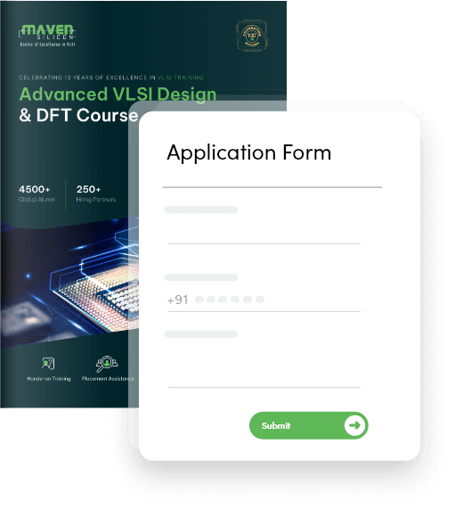
            Free VLSI Brochure

            Experience the immersive Advanced VLSI Design and DFT Course with 100% placement assistance

            Get the latest VLSI & Embedded Systems news, updates, technical and interview resources

            Subscribe to our Blog

            Have Doubts?
            FAQ

            Don't see your questions answered here?